Transistors and Logic Gates
Estimated reading time: .
An overview of how transistors work and how they can be assembled into Boolean logic elements.
ContentsI studied Computer Engineering, which involved a good number of Electrical Engineering classes, but I’m not an Electrical Engineer and it’s not really my strength. I’ll do my best to discuss them, but don’t expect the same depth I’ll give the actual computing articles.
Basic Principles
Short version: transistors are light switches. Each controls one light bulb, and when looking at light bulbs you can decide whether to flick other lights on or off. The end pattern of glowing and dim light bulbs is your output. If you assign meaning to individual bulbs and a deterministic instruction to how you switch lights on and off, you have a computer.
Imagine transistors as light-sensitive light switches, which turn on or off according to how much light is hitting them, and you’re pretty much there.
Electrical Operation
A transistor is essentially a switch that can be controlled by voltage signals. There are two main kinds: [bipolar junction transistors][bjt] and [field effect transistors][fet]. Both types can be further subclassified by material and behavior, but their overall behavior is the same: a voltage signal at the center terminal, called the Base for BJT and the Gate for FET, affects the electrical properties of the transistor to either permit or deny current passage between Collector and Emitter (BJT) or Source and Drain (FET).
I don’t have as strong of an understanding of transistors and electrical science as I do the computation topics, so I can’t really provide an explanation in between over-simplification and highly technical, but I’ll give it a shot.
The transistors used in modern computing devices are Metal Oxide Semiconductor Field Effect Transistors, or MOSFETs. They are made of a silicon base layer, which has regions that are doped with other metals. Doping, the sprinkling of impurities in the pure silicon, affects the electrical properties of the silicon.
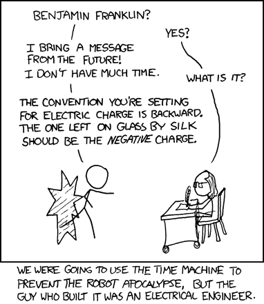
Benjamin Franklin got it wrong, so electrons have negative charge. However, convention says we measure current as flowing from positive regions to negative regions, so technically when we look at current flow, the “charge carrier” is a “hole”, and they flow as electrons jump in the opposite direction.
So, actually, higher voltages have fewer electrons than do lower voltages. Try not to think about it too much; just accept that everything works and move forward. That’s what we did in class, anyway.
Look there’s really no way to say this without a whiteboard. But at least you should get this XKCD now:
Logical Signaling
Since there are two electrical charges, there are two flavors of transistor layout: PNP and NPN. These terms simply refer to whether the primary channel is positively doped (by atoms with fewer than four valence electrons, such as boron or gallium) or negatively doped (by atoms with more than four valence electrons, such as phosphorus or arsenic). The substrate (base layer) is doped the other way, so PNP refers to P-doped source and drain terminals in an N-doped substrate, and vice versa for NPN.
The electrical properties of the differently doped regions inhibit electron flow by default. The voltage on the gate terminal, which is separated from the substrate by a thin oxide layer, must be significantly altered from the default voltage state in order for the gate’s electrical field to create an effect in the substrate that allows for current flow between source and drain.
The transistor is built with a metal-oxide material that sometimes conducts, by using an electrical field effect. Hence the name metal-oxide semiconductor field effect transistor.
NPN transistors require a gate voltage of +5V to activate (more or less), and shut off at 0V. PNP transistors require a gate voltage of 0V to activate (also more or less), and shut off at +5V. The former are active-high, and the latter are active-low.
This is important because MOSFETs work best when their activation signal is the opposite voltage from the voltage on the primary rail that they are switching.
What do I mean by primary rail? Transistors operate by connecting a signal path to either VCC (+5V) or GND (0V). These are called “primary rails”, and are directly connected to the main power supply (VCC) and main power sink (GND). This signal path fluctuates between 0 and 5 volts, so current flows from the VCC supply into the signal pathway, and from the signal pathway to the GND drain. So PNP transistors connect VCC to signal, and turn on when their control gate goes low (active-low) and NPN transistors connect signal to GND, and turn on when their control gate goes high (active-high).
Logic Gates
There are three general classes of transistor logic: PMOS, NMOS, and CMOS. The first letter of the name indicates the type of transistors used: PNP, NPN, and Combined.
In PMOS and NMOS, the transistor sits between their respective voltage target and the signal pathway. The signal pathway is connected directly to the other rail, so that when the transistors are off, the signal pathway is opposite, and when the transistors are on, they flood the signal with their own voltage level.
For instance, in NMOS logic, the signal pathway floats at high voltage when the transistor is turned off, and when the transistor turns on, the signal pathway is pulled to GND. In PMOS logic, the signal pathway floats at ground voltage when the transistor is turned off, and when the transistor turns on, the signal pathway is pulled to VCC.
In CMOS, both transistor types are used. This causes cleaner transitions between states, because the PMOS and NMOS transistors work opposite each other, so one is always actively pulling voltage.
Say you have a signal, \(A\), controlling an output \(Y\). Let us suppose that this is a NOT gate, so that when \(A\) is high \(Y\) is low, and when \(A\) is low \(Y\) is high. We know that NMOS transistors turn on with a high control voltage, and work best when passing a low voltage; we know that PMOS transistors turn on with a low control voltage, and work best when passing a high voltage. Thus, this NOT gate requires two transistors: a PMOS sitting between VCC and \(Y\), and an NMOS sitting between \(Y\) and GND.
When \(A\) goes high, the PMOS turns off and the NMOS turns on. Current freely flows from \(Y\) to GND, causing \(Y\) to quickly reach 0V. Thus, \(A\) is high and \(Y\) is low.
Then \(A\) abruptly goes low. The NMOS slowly shuts off, but the PMOS immediately turns on. This causes a connection between VCC and \(Y\) (and a little leakage to GND before the NMOS finishes shutting down), and \(Y\) jumps to 5V. Thus, \(A\) is low and \(Y\) is high.
The same principle works to build NAND gates and NOR gates: give the \(A\) and \(B\) input signals each a PMOS and an NMOS transistor, and set them up so that one side is in series while the other is in parallel. With the PMOS in series and NMOS in parallel, the output \(Y\) will be high only when \(A\) and \(B\) are both low (turning on the PMOS transistors, connecting VCC to Y), whereas if either \(A\) or \(B\) are high, then the PMOS pathway breaks and one of the NMOS pathways connects, pulling \(Y\) low. This is a NOR gate. Switch to PMOS in parallel and NMOS in series, and we have a NAND gate that will output high when either \(A\) or \(B\) is low, and will only output low when both \(A\) and \(B\) are high.
Conclusion
Since NAND and NOR are each functionally-complete logic elements, we can chain together their simple CMOS implementations into the Boolean primitives using other design laws into which I do not plan to descend at this time, and from there we can use Boolean algebra to design hardware that implements mathematics.
The essence of processor hardware design is this: at present, CMOS transistors are the atomic unit of signal switching. We can compose the Boolean primitives out of CMOS transistors, and then compose basic computation circuitry from those primitives, and then compose more advanced circuitry from the basic pieces.
Digital design is a fractal of composition, assembling high-level components out of lower-level components, which are themselves composed. Since everything above the Boolean primitives is constructed based on laws of mathematics, future changes to the structure of signal switching need only rearrange how the Boolean logical primitives are assembled from the electronic structures. Once the new elements are in place, everything else can switch over seamlessly.
Also, thanks to the layers of abstraction in digital design, knowledge of the electrical behavior of transistors is going to be wholly irrelevant (almost) to every other article in this series. You don’t need to read this, or if you did read it you don’t need to understand everything in it. If you did, though, good. More information never hurt.
Unfortunately I can’t find any images of transistor layouts that I like enough to use here. I personally find that, outside of textbooks, the best depiction of CMOS logic I’ve seen has been in this book. The book is basically a much better version of this series, but on the other hand, this blog series isn’t $14 for the ebook.
I highly recommend the book if you really want to get more into this stuff. It’s responsible for a good deal of my own understanding on the topic, so I would feel remiss if I didn’t plug it, especially on this particular article.
[bipolar junction transistors]: https://en.wikipedia.org/wiki/Bipolar_junction_transistor
[field effect transistors]: https://en.wikipedia.org/wiki/Field-effect_transistor
[xkcd_img]: https://imgs.xkcd.com/comics/urgent_mission.png “XKCD #567, where an electrical engineer travels back in time to tell Ben Franklin to switch the labels on his “positive” and “negative” jars”